Digital Systems tenth edition - Tocci - Chapter 3 - Solutions - 10 ed
3-1.*Draw the output waveform for the OR gate of Figure 3-52.

3-2. Suppose that the A input in Figure 3-52 is unintentionally shorted to ground (i.e., A 0). Draw the resulting output waveform.
3-3.*Suppose that the A input in Figure 3-52 is unintentionally shorted to the 5 V supply line (i.e., A 1). Draw the resulting output waveform.
3-4. Read the statements below concerning an OR gate.At first, they may appear to be valid,but after some thought you should realize that neither one is alwaystrue.Prove this by showing a specific example to refute each statement. (a) If the output waveform from an OR gate is the same as the waveform at one of its inputs, the other input is being held permanently LOW. (b) If the output waveform from an OR gate is always HIGH,one of its inputs is being held permanently HIGH.
3-5. How many different sets of input conditions will produce a HIGH output from a five-input OR gate?
3-6. Change the OR gate in Figure 3-52 to an AND gate. (a)*Draw the output waveform. (b) Draw the output waveform if the A input is permanently shorted to ground. (c) Draw the output waveform if A is permanently shorted to 5 V.
3-7.*Refer to Figure 3-4. Modify the circuit so that the alarm is to be activated only when the pressure and the temperature exceed their maximum limits at the same time.
3-8.*Change the OR gate in Figure 3-6 to an AND gate and draw the output waveform.
3-9. Suppose that you have an unknown two-input gate that is either an OR gate or an AND gate.What combination of input levels should you apply to the gate’s inputs to determine which type of gate it is?
3-10. True or false: No matter how many inputs it has, an AND gate will produce a HIGH output for only one combination of input levels.
3-11. Apply the A waveform from Figure 3-23to the input of an INVERTER. Draw the output waveform. Repeat for waveform B.
3-12. (a)* Write the Boolean expression for output x in Figure 3-53(a). Determine the value of x for all possible input conditions, and list the values in a truth table. (b) Repeat for the circuit in Figure 3-53(b).

3-13.*Create a complete analysis table for the circuit of Figure 3-15(b) by finding the logic levels present at each gate output for each of the 32 possible input combinations.
3-14. (a)*Change each OR to an AND, and each AND to an OR, in Figure 3-15(b).Then write the expression for the output. (b) Complete an analysis table.
3-15. Create a complete analysis table for the circuit of Figure 3-16 by finding the logic levels present at each gate output for each of the 16 possible combinations of input levels.
3-16. For each of the following expressions, construct the corresponding logic circuit, using AND and OR gates and INVERTERs.


3-17. *(a) Apply the input waveforms of Figure 3-54to a NOR gate,and draw the output waveform. (b) Repeat with C held permanently LOW. (c) Repeat with C held HIGH.

3-18. Repeat Problem 3-17 for a NAND gate.
3-19.*Write the expression for the output of Figure 3-55, and use it to determine the complete truth table.Then apply the waveforms of Figure 3-54 to the circuit inputs, and draw the resulting output waveform.

3-20. Determine the truth table for the circuit of Figure 3-24.
3-21. Modify the circuits that were constructed in Problem 3-16 so that NAND gates and NOR gates are used wherever appropriate.
3-22. Prove theorems (15a) and (15b) by trying all possible cases.
3-23.*DRILL QUESTION Complete each expression.

3-24. (a)*Simplify the following expression using theorems (13b),(3),and (4):

(b) Simplify the following expression using theorems (13a),(8),and (6):

3-25. Prove DeMorgan’s theorems by trying all possible cases.
3-26. Simplify each of the following expressions using DeMorgan’s theorems

3-27.*Use DeMorgan’s theorems to simplify the expression for the output of Figure 3-55.
3-28. Convert the circuit of Figure 3-53(b) to one using only NAND gates. Then write the output expression for the new circuit,simplify it using DeMorgan’s theorems, and compare it with the expression for the original circuit.
3-29. Convert the circuit of Figure 3-53(a) to one using only NOR gates. Then write the expression for the new circuit, simplify it using DeMorgan’s theorems, and compare it with the expression for the original circuit.
3-30. Show how a two-input NAND gate can be constructed from two-input NOR gates.
3-31. Show how a two-input NOR gate can be constructed from two-input NAND gates.
3-32. A jet aircraft employs a system for monitoring the rpm, pressure, and temperature values of its engines using sensors that operate as follows:
RPM sensor output = 0 only when speed 6 4800 rpm
P sensor output = 0 only when pressure 6 220 psi
T sensor output = 0 only when temperature 6 200°F
Figure 3-56 shows the logic circuit that controls a cockpit warning light for certain combinations of engine conditions.Assume that a HIGH at output W activates the warning light. (a)*Determine what engine conditions will give a warning to the pilot. (b) Change this circuit to one using all NAND gates.

3-33. For each statement below, draw the appropriate logic-gate symbol— standard or alternate—for the given operation. (a) A HIGH output occurs only when all three inputs are LOW. (b) A LOW output occurs when any of the four inputs is LOW. (c) A LOW output occurs only when all eight inputs are HIGH.
3-34. Draw the standard representations for each of the basic logic gates. Then draw the alternate representations.
3-35. The circuit of Figure 3-55 is supposed to be a simple digital combination lock whose output will generate an active-LOW signal for only one combination of inputs. (a)*Modify the circuit diagram so that it represents more effectively the circuit operation. (b) Use the new circuit diagram to determine the input combination that will activate the output. Do this by working back from the output using the information given by the gate symbols, as was done in Examples 3-22 and 3-23. Compare the results with the truth table obtained in Problem 3-19.
3-36. (a) Determine the input conditions needed to activate output Z in Figure 3-37(b). Do this by working back from the output, as was done in Examples 3-22 and 3-23. (b) Assume that it is the LOW state of Z that is to activate the alarm. Change the circuit diagram to reflect this, and then use the revised diagram to determine the input conditions needed to activate the alarm.
3-37. Modify the circuit of Figure 3-40 so that A1 0 is needed to produce DRIVE 1 instead of A1= 1.
3-38.*Determine the input conditions needed to cause the output in Figure 3-57 to go to its active state.

3-39.*What is the asserted state for the output of Figure 3-57? For the output of Figure 3-36(c)?
3-40. Use the results of Problem 3-38 to obtain the complete truth table for the circuit of Figure 3-57.
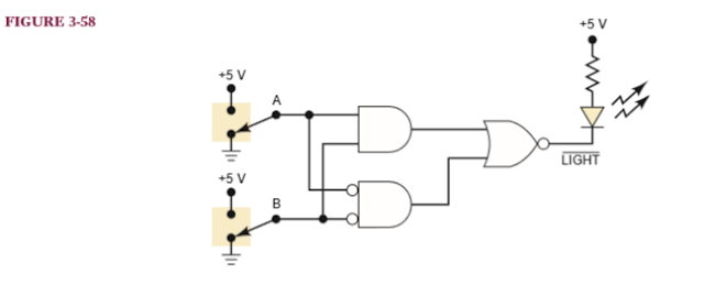
3-41.*Figure 3-58 shows an application of logic gates that simulates a twoway switch like the ones used in our homes to turn a light on or off from two different switches. Here the light is an LED that will be ON (conducting) when the NOR gate output is LOW.Note that this output is labeled to indicate that it is active-LOW. Determine the input conditions needed to turn on the LED.Then verify that the circuit operates as a two-way switch using switches A and B. (In Chapter 4, you will learn how to design circuits like this one to produce a given relationship between inputs and outputs.)
3-42. Redraw the circuits of (a)* Figure 3-57 and (b) Figure 3-58 using the IEEE/ANSI symbols.
3-43.*True or false: (a) VHDL is a computer programming language. (b) VHDL can accomplish the same thing as AHDL. (c) AHDL is an IEEE standard language. (d) Each intersection in a switch matrix can be programmed as an open or short circuit between a row and column wire. (e) The first item that appears at the top of an HDL listing is the functional description. (f) The type of an object indicates if it is an input or an output. (g) The mode of an object determines if it is an input or an output. (h) Buried nodes are nodes that have been deleted and will never be used again. (i) Local signals are another name for intermediate variables. (j) The header is a block of comments that document vital information about the project.
3-44. Redraw the programmable connection matrix from Figure 3-44.Label the output signals (horizontal lines) from the connection matrix (from top row to bottom row) as follows: AAABADHE. Draw an X in the appropriate intersections to short-circuit a row to a column and create these connections to the logic circuit.
Get 3.44 exercise solution
3-45.*Write the HDL code in the language of your choice that will produce the following output functions:
X = A+ B
Y= AB
Z= A+ B+ C
3-46. Write the HDL code in the language of your choice that will implement the logic circuit of Figure 3-39. (a) Use a single Boolean equation. (b) Use the intermediate variables V, W, X, and Y.
3-47.*Refer to Figure 3-40 in Example 3-23.Inputs A7 through A0 are address inputs that are supplied to this circuit from outputs of the microprocessor chip in a microcomputer.The eight-bit address code A7 to A0 selects which device the microprocessor wants to activate.In Example 3-23, the required address code to activate the disk drive was A7 through A0 = 111111102 = FE16. Modify the circuit so that the microprocessor must supply an address code of 4A16 to activate the disk drive.
3-48. Show how can be implemented with one two-input NOR and one two-input NAND gate.
3-49.*Implement y ABCD using only two-input NAND gates.

3-3.*Suppose that the A input in Figure 3-52 is unintentionally shorted to the 5 V supply line (i.e., A 1). Draw the resulting output waveform.
3-4. Read the statements below concerning an OR gate.At first, they may appear to be valid,but after some thought you should realize that neither one is alwaystrue.Prove this by showing a specific example to refute each statement. (a) If the output waveform from an OR gate is the same as the waveform at one of its inputs, the other input is being held permanently LOW. (b) If the output waveform from an OR gate is always HIGH,one of its inputs is being held permanently HIGH.
3-5. How many different sets of input conditions will produce a HIGH output from a five-input OR gate?
3-6. Change the OR gate in Figure 3-52 to an AND gate. (a)*Draw the output waveform. (b) Draw the output waveform if the A input is permanently shorted to ground. (c) Draw the output waveform if A is permanently shorted to 5 V.
3-7.*Refer to Figure 3-4. Modify the circuit so that the alarm is to be activated only when the pressure and the temperature exceed their maximum limits at the same time.
3-8.*Change the OR gate in Figure 3-6 to an AND gate and draw the output waveform.
3-9. Suppose that you have an unknown two-input gate that is either an OR gate or an AND gate.What combination of input levels should you apply to the gate’s inputs to determine which type of gate it is?
3-10. True or false: No matter how many inputs it has, an AND gate will produce a HIGH output for only one combination of input levels.
3-11. Apply the A waveform from Figure 3-23to the input of an INVERTER. Draw the output waveform. Repeat for waveform B.
3-12. (a)* Write the Boolean expression for output x in Figure 3-53(a). Determine the value of x for all possible input conditions, and list the values in a truth table. (b) Repeat for the circuit in Figure 3-53(b).

3-13.*Create a complete analysis table for the circuit of Figure 3-15(b) by finding the logic levels present at each gate output for each of the 32 possible input combinations.
3-14. (a)*Change each OR to an AND, and each AND to an OR, in Figure 3-15(b).Then write the expression for the output. (b) Complete an analysis table.
3-15. Create a complete analysis table for the circuit of Figure 3-16 by finding the logic levels present at each gate output for each of the 16 possible combinations of input levels.
3-16. For each of the following expressions, construct the corresponding logic circuit, using AND and OR gates and INVERTERs.
3-17. *(a) Apply the input waveforms of Figure 3-54to a NOR gate,and draw the output waveform. (b) Repeat with C held permanently LOW. (c) Repeat with C held HIGH.

3-18. Repeat Problem 3-17 for a NAND gate.
3-19.*Write the expression for the output of Figure 3-55, and use it to determine the complete truth table.Then apply the waveforms of Figure 3-54 to the circuit inputs, and draw the resulting output waveform.

3-21. Modify the circuits that were constructed in Problem 3-16 so that NAND gates and NOR gates are used wherever appropriate.
3-22. Prove theorems (15a) and (15b) by trying all possible cases.
3-23.*DRILL QUESTION Complete each expression.

3-24. (a)*Simplify the following expression using theorems (13b),(3),and (4):

(b) Simplify the following expression using theorems (13a),(8),and (6):

3-26. Simplify each of the following expressions using DeMorgan’s theorems

3-27.*Use DeMorgan’s theorems to simplify the expression for the output of Figure 3-55.
3-28. Convert the circuit of Figure 3-53(b) to one using only NAND gates. Then write the output expression for the new circuit,simplify it using DeMorgan’s theorems, and compare it with the expression for the original circuit.
3-29. Convert the circuit of Figure 3-53(a) to one using only NOR gates. Then write the expression for the new circuit, simplify it using DeMorgan’s theorems, and compare it with the expression for the original circuit.
3-30. Show how a two-input NAND gate can be constructed from two-input NOR gates.
3-31. Show how a two-input NOR gate can be constructed from two-input NAND gates.
3-32. A jet aircraft employs a system for monitoring the rpm, pressure, and temperature values of its engines using sensors that operate as follows:
RPM sensor output = 0 only when speed 6 4800 rpm
P sensor output = 0 only when pressure 6 220 psi
T sensor output = 0 only when temperature 6 200°F
Figure 3-56 shows the logic circuit that controls a cockpit warning light for certain combinations of engine conditions.Assume that a HIGH at output W activates the warning light. (a)*Determine what engine conditions will give a warning to the pilot. (b) Change this circuit to one using all NAND gates.

3-33. For each statement below, draw the appropriate logic-gate symbol— standard or alternate—for the given operation. (a) A HIGH output occurs only when all three inputs are LOW. (b) A LOW output occurs when any of the four inputs is LOW. (c) A LOW output occurs only when all eight inputs are HIGH.
3-34. Draw the standard representations for each of the basic logic gates. Then draw the alternate representations.
3-35. The circuit of Figure 3-55 is supposed to be a simple digital combination lock whose output will generate an active-LOW signal for only one combination of inputs. (a)*Modify the circuit diagram so that it represents more effectively the circuit operation. (b) Use the new circuit diagram to determine the input combination that will activate the output. Do this by working back from the output using the information given by the gate symbols, as was done in Examples 3-22 and 3-23. Compare the results with the truth table obtained in Problem 3-19.
3-36. (a) Determine the input conditions needed to activate output Z in Figure 3-37(b). Do this by working back from the output, as was done in Examples 3-22 and 3-23. (b) Assume that it is the LOW state of Z that is to activate the alarm. Change the circuit diagram to reflect this, and then use the revised diagram to determine the input conditions needed to activate the alarm.
3-37. Modify the circuit of Figure 3-40 so that A1 0 is needed to produce DRIVE 1 instead of A1= 1.
3-38.*Determine the input conditions needed to cause the output in Figure 3-57 to go to its active state.

3-40. Use the results of Problem 3-38 to obtain the complete truth table for the circuit of Figure 3-57.
3-41.*Figure 3-58 shows an application of logic gates that simulates a twoway switch like the ones used in our homes to turn a light on or off from two different switches. Here the light is an LED that will be ON (conducting) when the NOR gate output is LOW.Note that this output is labeled to indicate that it is active-LOW. Determine the input conditions needed to turn on the LED.Then verify that the circuit operates as a two-way switch using switches A and B. (In Chapter 4, you will learn how to design circuits like this one to produce a given relationship between inputs and outputs.)

3-42. Redraw the circuits of (a)* Figure 3-57 and (b) Figure 3-58 using the IEEE/ANSI symbols.
3-43.*True or false: (a) VHDL is a computer programming language. (b) VHDL can accomplish the same thing as AHDL. (c) AHDL is an IEEE standard language. (d) Each intersection in a switch matrix can be programmed as an open or short circuit between a row and column wire. (e) The first item that appears at the top of an HDL listing is the functional description. (f) The type of an object indicates if it is an input or an output. (g) The mode of an object determines if it is an input or an output. (h) Buried nodes are nodes that have been deleted and will never be used again. (i) Local signals are another name for intermediate variables. (j) The header is a block of comments that document vital information about the project.
3-44. Redraw the programmable connection matrix from Figure 3-44.Label the output signals (horizontal lines) from the connection matrix (from top row to bottom row) as follows: AAABADHE. Draw an X in the appropriate intersections to short-circuit a row to a column and create these connections to the logic circuit.
Get 3.44 exercise solution
3-45.*Write the HDL code in the language of your choice that will produce the following output functions:
X = A+ B
Y= AB
Z= A+ B+ C
3-46. Write the HDL code in the language of your choice that will implement the logic circuit of Figure 3-39. (a) Use a single Boolean equation. (b) Use the intermediate variables V, W, X, and Y.
3-47.*Refer to Figure 3-40 in Example 3-23.Inputs A7 through A0 are address inputs that are supplied to this circuit from outputs of the microprocessor chip in a microcomputer.The eight-bit address code A7 to A0 selects which device the microprocessor wants to activate.In Example 3-23, the required address code to activate the disk drive was A7 through A0 = 111111102 = FE16. Modify the circuit so that the microprocessor must supply an address code of 4A16 to activate the disk drive.
3-48. Show how can be implemented with one two-input NOR and one two-input NAND gate.
3-49.*Implement y ABCD using only two-input NAND gates.
Digital Systems tenth edition - Tocci - Chapter 2 - Solutions - 10 ed
2-1. Convert these binary numbers to decimal. (a)*10110 (d) 01101011 (g)*1111010111 (b) 10010101 (e)*11111111 (h) 11011111 (c)*100100001001 (f) 01101111
2-2. Convert the following decimal values to binary. (a)*37 (d) 1000 (g)*205 (b) 13 (e)*77 (h) 2133 (c)*189 (f) 390 (i)*511
2-3. What is the largest decimal value that can be represented by (a)* an eight-bit binary number? (b) A 16-bit number?
2-4. Convert each hex number to its decimal equivalent. (a)*743 (d) 2000 (g)*7FF (b) 36 (e)*165 (h) 1204 (c)*37FD (f) ABCD
2-5. Convert each of the following decimal numbers to hex. (a)*59 (d) 1024 (g)*65,536 (b) 372 (e)*771 (h) 255 (c)*919 (f) 2313
2-6. Convert each of the hex values from Problem 2-4 to binary.
2-7. Convert the binary numbers in Problem 2-1 to hex.
2-8. List the hex numbers in sequence from 19516 to 28016.
2-9. When a large decimal number is to be converted to binary, it is sometimes easier to convert it first to hex,and then from hex to binary.Try this procedure for 213310 and compare it with the procedure used in Problem 2-2(h).
2-10. How many hex digits are required to represent decimal numbers up to 20,000?
2-11. Convert these hex values to decimal. (a)*92 (d) ABCD (g)*2C0 (b) 1A6 (e)*000F (h) 7FF (c)*37FD (f) 55
2-12. Convert these decimal values to hex. (a)*75 (d) 24 (g)*25,619 (b) 314 (e)*7245 (h) 4095 (c)*2048 (f) 498
2-13. Take each four-bit binary number in the order they are written and write the equivalent hex digit without performing a calculation by hand or by calculator. (a) 1001 (e) 1111 (i) 1011 (m) 0001 (b) 1101 (f) 0010 (j) 1100 (n) 0101 (c) 1000 (g) 1010 (k)0011 (o) 0111 (d) 0000 (h) 1001 (l) 0100 (p) 0110
2-14. Take each hex digit and write its four-bit binary value without performing any calculations by hand or by calculator. (a) 6 (e) 4 (i) 9 (m) 0 (b) 7 (f) 3 (j) A (n) 8 (c) 5 (g) C (k)2 (o) D (d) 1 (h) B (l) F (p) 9
2-15.* Convert the binary numbers in Problem 2-1 to hexadecimal.
2-16.* Convert the hex values in Problem 2-11 to binary.
2-17.* List the hex numbers in sequence from 280 to 2A0.
2-18. How many hex digits are required to represent decimal numbers up to 1 million?
2-19. Encode these decimal numbers in BCD. (a)*47 (d) 6727 (g) *89,627 (b) 962 (e)*13 (h)1024 (c)*187 (f) 529
2-20. How many bits are required to represent the decimal numbers in the range from 0 to 999 using (a) straight binary code? (b) Using BCD code?
2-21. The following numbers are in BCD. Convert them to decimal. (a)*1001011101010010 (d) 0111011101110101 (b) 000110000100 (e)*010010010010 (c)*011010010101 (f) 010101010101
2-22.*(a) How many bits are contained in eight bytes? (b) What is the largest hex number that can be represented in four bytes? (c) What is the largest BCD-encoded decimal value that can be represented in three bytes?
2-23. (a) Refer to Table 2-4.What is the most significant nibble of the ASCII code for the letter X? (b) How many nibbles can be stored in a 16-bit word? (c) How many bytes does it take to make up a 24-bit word?
2-24. Represent the statement “ ” in ASCII code. Attach an oddparity bit.
2-25.*Attach an even-parity bit to each of the ASCII codes for Problem 2-24, and give the results in hex.
2-26. The following bytes (shown in hex) represent a person’s name as it would be stored in a computer’s memory.Each byte is a padded ASCII code. Determine the name of each person. (a)*42 45 4E 20 53 4D 49 54 48 (b) 4A 6F 65 20 47 72 65 65 6E
2-27. Convert the following decimal numbers to BCD code and then attach an odd parity bit. (a)*74 (c)*8884 (e)*165 (b) 38 (d) 275 (f) 9201
2-28.*In a certain digital system, the decimal numbers from 000 through 999 are represented in BCD code.An odd-parity bit is also included at the end of each code group. Examine each of the code groups below, and assume that each one has just been transferred from one location to another. Some of the groups contain errors. Assume that no more than two errors have occurred for each group.Determine which of the code groups have a single error and which of them definitely have a double error. (Hint: Remember that this is a BCD code.)
(a) 1001010110000
parity bit
(b) 0100011101100 (c) 0111110000011 (d) 1000011000101
2-29. Suppose that the receiver received the following data from the transmitter of Example 2-16:
0 1 0 0 1 0 0 0
1 1 0 0 0 1 0 1
1 1 0 0 1 1 0 0
1 1 0 0 1 0 0 0
1 1 0 0 1 1 0 0
What errors can the receiver determine in these received data?
2-30.*Perform each of the following conversions.For some of them,you may want to try several methods to see which one works best for you. For example, a binary-to-decimal conversion may be done directly, or it may be done as a binary-to-hex conversion followed by a hex-todecimal conversion. (a) 141710 _____ 2 (b) 25510 _____ 2 (c) 110100012 _____ 10 (d) 11101010001001112 _____ 10
2-31.*Represent the decimal value 37 in each of the following ways. (a) straight binary (b) BCD (c) hex (d) ASCII (i.e., treat each digit as a character)
2-32.*Fill in the blanks with the correct word or words. (a) Conversion from decimal to _____ requires repeated division by 16. (b) Conversion from decimal to binary requires repeated division by _____. (c) In the BCD code, each _____ is converted to its four-bit binary equivalent. (d) The _____ code has the characteristic that only one bit changes in going from one step to the next. (e) A transmitter attaches a _____ to a code group to allow the receiver to detect _____. (f) The _____ code is the most common alphanumeric code used in computer systems. (g) _____ is often used as a convenient way to represent large binary numbers. (h) A string of eight bits is called a _____.
2-33. Write the binary number that results when each of the following numbers is incremented by one. (a)*0111 (b) 010011 (c) 1011
2-34. Decrement each binary number. (a)*1110 (b) 101000 (c) 1110
2-35. Write the number that results when each of the following is incremented. (a)*777916 (c)*OFFF16 (e)*9FF16 (b) 999916 (d) 200016 (f) 100A16
2-36.*Repeat Problem 2-35 for the decrement operation.
2-37.*In a microcomputer, the addresses of memory locations are binary numbers that identify each memory circuit where a byte is stored.The number of bits that make up an address depends on how many memory locations there are.Since the number of bits can be very large,the addresses are often specified in hex instead of binary. (a) If a microcomputer uses a 20-bit address, how many different memory locations are there? (b) How many hex digits are needed to represent the address of a memory location? (c) What is the hex address of the 256th memory location? (Note:The first address is always 0.)
2-38. In an audio CD, the audio voltage signal is typically sampled about 44,000 times per second, and the value of each sample is recorded on the CD surface as a binary number. In other words, each recorded binary number represents a single voltage point on the audio signal waveform. (a) If the binary numbers are six bits in length, how many different voltage values can be represented by a single binary number? Repeat for eight bits and ten bits. (b) If ten-bit numbers are used,how many bits will be recorded on the CD in 1 second? (c) If a CD can typically store 5 billion bits, how many seconds of audio can be recorded when ten-bit numbers are used?
2-39.*A black-and-white digital camera lays a fine grid over an image and then measures and records a binary number representing the level of gray it sees in each cell of the grid. For example, if four-bit numbers are used, the value of black is set to 0000 and the value of white to 1111, and any level of gray is somewhere between 0000 and 1111. If six-bit numbers are used, black is 000000, white is 111111, and all grays are between the two. Suppose we wanted to distinguish among 254 different levels of gray within each cell of the grid. How many bits would we need to use to represent these levels?
2-40. A 3-Megapixel digital camera stores an eight-bit number for the brightness of each of the primary colors (red, green, blue) found in each picture element (pixel). If every bit is stored (no data compression), how many pictures can be stored on a 128-Megabyte memory card? (Note: In digital systems, Mega means 220.)
2-2. Convert the following decimal values to binary. (a)*37 (d) 1000 (g)*205 (b) 13 (e)*77 (h) 2133 (c)*189 (f) 390 (i)*511
2-3. What is the largest decimal value that can be represented by (a)* an eight-bit binary number? (b) A 16-bit number?
2-4. Convert each hex number to its decimal equivalent. (a)*743 (d) 2000 (g)*7FF (b) 36 (e)*165 (h) 1204 (c)*37FD (f) ABCD
2-5. Convert each of the following decimal numbers to hex. (a)*59 (d) 1024 (g)*65,536 (b) 372 (e)*771 (h) 255 (c)*919 (f) 2313
2-6. Convert each of the hex values from Problem 2-4 to binary.
2-7. Convert the binary numbers in Problem 2-1 to hex.
2-8. List the hex numbers in sequence from 19516 to 28016.
2-9. When a large decimal number is to be converted to binary, it is sometimes easier to convert it first to hex,and then from hex to binary.Try this procedure for 213310 and compare it with the procedure used in Problem 2-2(h).
2-10. How many hex digits are required to represent decimal numbers up to 20,000?
2-11. Convert these hex values to decimal. (a)*92 (d) ABCD (g)*2C0 (b) 1A6 (e)*000F (h) 7FF (c)*37FD (f) 55
2-12. Convert these decimal values to hex. (a)*75 (d) 24 (g)*25,619 (b) 314 (e)*7245 (h) 4095 (c)*2048 (f) 498
2-13. Take each four-bit binary number in the order they are written and write the equivalent hex digit without performing a calculation by hand or by calculator. (a) 1001 (e) 1111 (i) 1011 (m) 0001 (b) 1101 (f) 0010 (j) 1100 (n) 0101 (c) 1000 (g) 1010 (k)0011 (o) 0111 (d) 0000 (h) 1001 (l) 0100 (p) 0110
2-14. Take each hex digit and write its four-bit binary value without performing any calculations by hand or by calculator. (a) 6 (e) 4 (i) 9 (m) 0 (b) 7 (f) 3 (j) A (n) 8 (c) 5 (g) C (k)2 (o) D (d) 1 (h) B (l) F (p) 9
2-15.* Convert the binary numbers in Problem 2-1 to hexadecimal.
2-16.* Convert the hex values in Problem 2-11 to binary.
2-17.* List the hex numbers in sequence from 280 to 2A0.
2-18. How many hex digits are required to represent decimal numbers up to 1 million?
2-19. Encode these decimal numbers in BCD. (a)*47 (d) 6727 (g) *89,627 (b) 962 (e)*13 (h)1024 (c)*187 (f) 529
2-20. How many bits are required to represent the decimal numbers in the range from 0 to 999 using (a) straight binary code? (b) Using BCD code?
2-21. The following numbers are in BCD. Convert them to decimal. (a)*1001011101010010 (d) 0111011101110101 (b) 000110000100 (e)*010010010010 (c)*011010010101 (f) 010101010101
2-22.*(a) How many bits are contained in eight bytes? (b) What is the largest hex number that can be represented in four bytes? (c) What is the largest BCD-encoded decimal value that can be represented in three bytes?
2-23. (a) Refer to Table 2-4.What is the most significant nibble of the ASCII code for the letter X? (b) How many nibbles can be stored in a 16-bit word? (c) How many bytes does it take to make up a 24-bit word?
2-24. Represent the statement “ ” in ASCII code. Attach an oddparity bit.
2-25.*Attach an even-parity bit to each of the ASCII codes for Problem 2-24, and give the results in hex.
2-26. The following bytes (shown in hex) represent a person’s name as it would be stored in a computer’s memory.Each byte is a padded ASCII code. Determine the name of each person. (a)*42 45 4E 20 53 4D 49 54 48 (b) 4A 6F 65 20 47 72 65 65 6E
2-27. Convert the following decimal numbers to BCD code and then attach an odd parity bit. (a)*74 (c)*8884 (e)*165 (b) 38 (d) 275 (f) 9201
2-28.*In a certain digital system, the decimal numbers from 000 through 999 are represented in BCD code.An odd-parity bit is also included at the end of each code group. Examine each of the code groups below, and assume that each one has just been transferred from one location to another. Some of the groups contain errors. Assume that no more than two errors have occurred for each group.Determine which of the code groups have a single error and which of them definitely have a double error. (Hint: Remember that this is a BCD code.)
(a) 1001010110000
parity bit
(b) 0100011101100 (c) 0111110000011 (d) 1000011000101
0 1 0 0 1 0 0 0
1 1 0 0 0 1 0 1
1 1 0 0 1 1 0 0
1 1 0 0 1 0 0 0
1 1 0 0 1 1 0 0
What errors can the receiver determine in these received data?
2-30.*Perform each of the following conversions.For some of them,you may want to try several methods to see which one works best for you. For example, a binary-to-decimal conversion may be done directly, or it may be done as a binary-to-hex conversion followed by a hex-todecimal conversion. (a) 141710 _____ 2 (b) 25510 _____ 2 (c) 110100012 _____ 10 (d) 11101010001001112 _____ 10
2-31.*Represent the decimal value 37 in each of the following ways. (a) straight binary (b) BCD (c) hex (d) ASCII (i.e., treat each digit as a character)
2-32.*Fill in the blanks with the correct word or words. (a) Conversion from decimal to _____ requires repeated division by 16. (b) Conversion from decimal to binary requires repeated division by _____. (c) In the BCD code, each _____ is converted to its four-bit binary equivalent. (d) The _____ code has the characteristic that only one bit changes in going from one step to the next. (e) A transmitter attaches a _____ to a code group to allow the receiver to detect _____. (f) The _____ code is the most common alphanumeric code used in computer systems. (g) _____ is often used as a convenient way to represent large binary numbers. (h) A string of eight bits is called a _____.
2-33. Write the binary number that results when each of the following numbers is incremented by one. (a)*0111 (b) 010011 (c) 1011
2-34. Decrement each binary number. (a)*1110 (b) 101000 (c) 1110
2-35. Write the number that results when each of the following is incremented. (a)*777916 (c)*OFFF16 (e)*9FF16 (b) 999916 (d) 200016 (f) 100A16
2-36.*Repeat Problem 2-35 for the decrement operation.
2-37.*In a microcomputer, the addresses of memory locations are binary numbers that identify each memory circuit where a byte is stored.The number of bits that make up an address depends on how many memory locations there are.Since the number of bits can be very large,the addresses are often specified in hex instead of binary. (a) If a microcomputer uses a 20-bit address, how many different memory locations are there? (b) How many hex digits are needed to represent the address of a memory location? (c) What is the hex address of the 256th memory location? (Note:The first address is always 0.)
2-38. In an audio CD, the audio voltage signal is typically sampled about 44,000 times per second, and the value of each sample is recorded on the CD surface as a binary number. In other words, each recorded binary number represents a single voltage point on the audio signal waveform. (a) If the binary numbers are six bits in length, how many different voltage values can be represented by a single binary number? Repeat for eight bits and ten bits. (b) If ten-bit numbers are used,how many bits will be recorded on the CD in 1 second? (c) If a CD can typically store 5 billion bits, how many seconds of audio can be recorded when ten-bit numbers are used?
2-39.*A black-and-white digital camera lays a fine grid over an image and then measures and records a binary number representing the level of gray it sees in each cell of the grid. For example, if four-bit numbers are used, the value of black is set to 0000 and the value of white to 1111, and any level of gray is somewhere between 0000 and 1111. If six-bit numbers are used, black is 000000, white is 111111, and all grays are between the two. Suppose we wanted to distinguish among 254 different levels of gray within each cell of the grid. How many bits would we need to use to represent these levels?
2-40. A 3-Megapixel digital camera stores an eight-bit number for the brightness of each of the primary colors (red, green, blue) found in each picture element (pixel). If every bit is stored (no data compression), how many pictures can be stored on a 128-Megabyte memory card? (Note: In digital systems, Mega means 220.)
Digital Systems tenth edition - Tocci - Chapter1 - Solutions - 10 ed
1-1.*Which of the following are analog quantities, and which are digital? (a) Number of atoms in a sample of material (b) Altitude of an aircraft (c) Pressure in a bicycle tire (d) Current through a speaker (e) Timer setting on a microwave oven
1-2. Which of the following are analog quantities, and which are digital? (a) Width of a piece of lumber (b) The amount of time before the oven buzzer goes off (c) The time of day displayed on a quartz watch (d) Altitude above sea level measured on a staircase (e) Altitude above sea level measured on a ramp
1-3.*Convert the following binary numbers to their equivalent decimal values. (a) 110012 (b) 1001.10012 (c) 10011011001.101102
1-4. Convert the following binary numbers to decimal. (a) 100112 (b) 1100.0101 (c) 10011100100.10010
1-5.*Using three bits, show the binary counting sequence from 000 to 111.
1-6. Using six bits, show the binary counting sequence from 000000 to 111111.
1-7.*What is the maximum number that we can count up to using 10 bits?
1-8. What is the maximum number that we can count up to using 14 bits?
1-9.*How many bits are needed to count up to a maximum of 511?
1-10. How many bits are needed to count up to a maximum of 63?
1-11.*Draw the timing diagram for a digital signal that continuously alternates between 0.2 V (binary 0) for 2 ms and 4.4 V (binary 1) for 4 ms.
1-12. Draw the timing diagram for a signal that alternates between 0.3 V (binary 0) for 5 ms and 3.9 V (binary 1) for 2 ms.
1-13.*Suppose that the decimal integer values from 0 to 15 are to be transmitted in binary. (a) How many lines will be needed if parallel representation is used? (b) How many will be needed if serial representation is used?
1-14. How is a microprocessor different from a microcomputer?
1-15. How is a microcontroller different from a microcomputer?
Subscribe to:
Posts (Atom)